On 17 November 2026 the Commerce Ministry reported that India's electronic goods exports grew 44% to USD 31.97 billion in April–September of FY 2026-27. Behind that figure sits a very small object: a chip of silicon, a few millimetres across, carrying billions of switches. Phones, radar sets, drone controllers and missile seekers all depend on it. CDS and NDA papers ask about it almost every year. The science is one idea repeated three times: control the carriers in a crystal (doping), join two kinds of crystal (the p-n junction), then add a third layer (the transistor).
Conductor, Insulator or Semiconductor: The Band Gap Decides
By Abhishek Thakur · Science faculty, The Cavalier · 15 years teaching NDA and CDS Science
In an isolated atom each electron has its own energy level. In a crystal the levels merge into bands. The band holding the outer (valence) electrons is the valence band. The empty band above it is the conduction band, and only electrons in it can carry current. The gap between the two is the energy band gap, Eg.
| Material | Band picture | Resistivity (Ω m) | Examples |
|---|---|---|---|
| Metal | Bands overlap or the conduction band is part-filled; Eg is about 0 | 10−8 to 10−2 | Copper, aluminium, tin |
| Semiconductor | Small gap, below about 3 eV; a few electrons cross at room temperature | 10−5 to 106 | Silicon, germanium, gallium arsenide |
| Insulator | Large gap, above about 3 eV; nothing crosses | 1011 to 1019 | Diamond, glass, rubber |
Carbon (diamond), silicon, germanium and tin all have four outer electrons, yet they behave differently, because of how tightly the bonding electrons are held. They sit in the second shell in carbon, the third in silicon, the fourth in germanium. The further out, the easier to free. So the band gap falls down the group: diamond 5.4 eV, silicon 1.1 eV, germanium 0.7 eV, tin about 0 eV. Diamond is an insulator, silicon and germanium are semiconductors, and tin is a metal.
Two features set a semiconductor apart. First, its resistance falls as temperature rises, the opposite of a metal, because heat lifts more electrons across the gap. Second, an electron that leaves a covalent bond leaves a vacancy called a hole, which behaves like a positive charge. A neighbouring electron can hop in, so the hole appears to move the other way. In a pure (intrinsic) crystal ne = nh = ni, and the current is an electron current plus a hole current. At absolute zero a pure semiconductor is an insulator.
The first transistors were germanium. Silicon took over because its devices tolerate higher voltages and currents and change less with temperature, and it is abundant. Both are metalloids: see where they sit on our periodic table page.
Doping: Making n-type and p-type Crystals
Pure silicon conducts too poorly to build devices. The cure is doping: adding a few atoms of impurity per million of silicon. The dopant must be about the size of a silicon atom, so that it fits the lattice undistorted.
| Feature | n-type | p-type |
|---|---|---|
| Dopant valency | Pentavalent (5 outer electrons): phosphorus, arsenic, antimony | Trivalent (3 outer electrons): boron, aluminium, indium |
| What happens | Four electrons bond; the fifth is almost free | One bond is left short of an electron: a hole |
| Dopant is called | Donor | Acceptor |
| Majority carriers | Electrons (ne ≫ nh) | Holes (nh ≫ ne) |
| Minority carriers | Holes | Electrons |
| Energy to free the carrier | About 0.05 eV in silicon, against 1.1 eV to break a bond | |
At room temperature nearly every donor has given up its electron, so the carrier count depends on how much you add and hardly at all on the weather.
An n-type crystal is not negatively charged. Each extra electron is balanced by the positive charge of the donor atom that gave it. Both n-type and p-type crystals stay electrically neutral. "n" and "p" name the majority carrier, not the net charge.
At a given temperature the product ne × nh equals ni2, a constant. Add many electrons and recombination mops up holes, so the minority count drops.
A silicon crystal has 5 × 1028 atoms per m³ and ni = 1.5 × 10¹⁶ m−3. It is doped with arsenic at 2 parts per million. Find the electron and hole densities.
The p-n Junction and the Diode
Grow a p-type region and an n-type region in one crystal and you get the p-n junction, the key to almost every device in this article. Holes diffuse from p to n, and electrons from n to p, because each is crowded on its home side. Each crossing carrier leaves behind a fixed, charged ion core. A thin slab around the junction loses its free carriers: the depletion region, less than a micrometre thick. Its fixed charges create a field that pushes carriers back (drift) until drift balances diffusion. The voltage across the slab is the barrier potential: about 0.7 V for silicon and 0.3 V for germanium.
A p-n junction with metal contacts is a diode. An outside battery can shrink or enlarge the barrier.
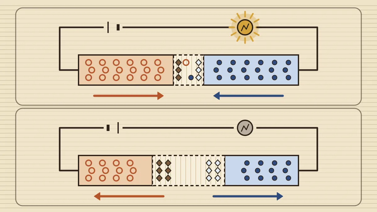
| Property | Forward bias | Reverse bias |
|---|---|---|
| Connection | p to positive terminal, n to negative | p to negative terminal, n to positive |
| Depletion region | Narrows | Widens |
| Barrier height | Falls, to V₀ − V | Rises, to V₀ + V |
| Current | Large, in milliamperes, rising steeply beyond the knee voltage | Tiny, microamperes or nanoamperes, from minority carriers (reverse saturation current) |
So a diode conducts one way and blocks the other. Its current–voltage graph is a curve, not a straight line, so a diode is non-ohmic. Push the reverse voltage high enough and the junction breaks down and current surges. That damages an ordinary diode, but a heavily doped Zener diode is built to run there: the voltage across it stays almost constant while current varies widely, which makes it a voltage regulator.
Rectification. Because a diode passes current in one direction only, it turns alternating current into direct current. A single diode in series with the load gives a half-wave rectifier, which passes one half of each cycle, so the output has the same frequency as the input. Two diodes on a centre-tapped transformer give a full-wave rectifier, which uses both halves, so the output ripple is twice the input frequency: a 50 Hz mains input gives 100 Hz.
One Junction, Many Jobs: LED, Photodiode, Solar Cell
Tune the doping and the junction does different work. All of the devices below are p-n junctions.
| Device | How it is used | What happens | Uses |
|---|---|---|---|
| Zener diode | Reverse bias, in breakdown | Holds a steady voltage | Voltage regulators |
| LED (light-emitting diode) | Forward bias | Electrons and holes recombine at the junction and release the energy as light | Bulbs, displays, indicators, remote controls |
| Photodiode | Reverse bias | Light creates electron-hole pairs; the reverse current rises with the intensity | Light sensors, optical-fibre receivers |
| Solar cell | No outside battery | Light creates pairs; the junction field separates them and drives a current | Panels, calculators, satellites |
LED. It turns electrical energy into light directly, with no filament to heat. The colour depends on the band gap of the material, because each recombination releases a photon of roughly that energy. Gallium arsenide gives infrared, as in TV remotes, gallium arsenide phosphide gives red, and gallium nitride gives blue. The Nobel Prize in Physics 2014 went to Isamu Akasaki, Hiroshi Amano and Shuji Nakamura for the blue LED, which made white LED lighting possible. LEDs are efficient, long-lived and low-voltage, and their reverse breakdown voltage is low, so they must not be connected backwards.
Photodiode versus solar cell. The photodiode is a detector, used in reverse bias, and its output follows the light intensity. The solar cell is a large-area generator that needs no battery. The photovoltaic effect is explained on our solar cells page.
A laser diode is a special LED that emits narrow, coherent light, used in barcode readers and optical drives.
From Diode to Transistor to Chip
Before the 1940s, amplifying a signal needed a vacuum tube, a hot, bulky glass bulb. In December 1947 John Bardeen and Walter Brattain, working with William Shockley at Bell Laboratories, made the first transistor. The three shared the 1956 Nobel Prize in Physics. The transistor does the same job in a speck of crystal, using little power and lasting far longer.
A transistor is a crystal with three layers: n-p-n or p-n-p. The three terminals are the emitter, the base and the collector.
| Region | Role | Doping and size |
|---|---|---|
| Emitter | Sends carriers into the base | Heavily doped |
| Base (the middle layer) | The control gate | Very thin and lightly doped, so most carriers pass straight through |
| Collector | Collects the carriers | The largest region, since it gets hot |
In normal use the emitter-base junction is forward biased and the collector-base junction is reverse biased. A small base current controls a much larger collector current. That is amplification: the ratio of collector to base current is the current gain. Driven fully off or fully on, it is a switch, and switches combine into logic gates: AND, OR and NOT, plus NAND and NOR, the universal gates, because any other gate can be built from either one alone.
Next came the integrated circuit: transistors, diodes and resistors made together on a single piece of silicon. Jack Kilby of Texas Instruments built the first in 1958 (Nobel Prize in Physics 2000). A modern chip holds billions of transistors on a slice the size of a fingernail, and the number on a chip has doubled about every two years, a trend called Moore's law.
A chip is made in three stages: design, fabrication (printing circuits on silicon wafers) and packaging and testing. The India Semiconductor Mission, approved in December 2021 with ₹76,000 crore, covers all three. Our notes on the Sanand packaging plant and the components scheme and Semicon 2.0 portal follow the factories. For defence the point is strategic: radars, communications and guidance all rest on chips.
How UPSC Has Asked It: Past Papers Solved
These are actual CDS and NDA questions since 2018. UPSC keeps this topic at the identify-the-device level, and the same ideas come back.
Which one of the following devices is non-ohmic?
(a) Conducting copper coil (b) Electric heating coil (c) Semiconductor diode (d) Rheostat
Answer: (c). A diode conducts well one way and barely the other, so its I–V graph is a curve and Ohm's law does not hold. The copper coil, heating coil and rheostat are all treated as ohmic conductors at a steady temperature.
Which one of the following does not convert electrical energy into light energy?
(a) A candle (b) A light-emitting diode (c) A laser (d) A television set
Answer: (a). A candle gives light by burning wax, which is chemical energy. The LED, the laser and the TV screen all start from electrical energy.
LED (a semi-conductor device) is an abbreviation that stands for
(a) Licence for Energy Detector (b) Light Energy Device (c) Light Emitting Diode (d) Lost Energy Detector
Answer: (c). NDA 2018-II (Q66) asked for the same full form. An LED is a p-n junction.
In which one of the following devices, the light energy is converted into the electrical energy?
(a) Light-emitting diode (b) Laser diode (c) Solar cell (d) Transistor
Answer: (c). The solar cell is the light-to-electricity device. The LED and laser diode run the other way (electricity to light), and a transistor amplifies or switches.
Which one of the following allotropes of carbon is isomorphous with crystalline silicon?
(a) Coke (b) Diamond (c) Graphite (d) Coal
Answer: (b). Diamond and crystalline silicon share the diamond-like lattice in which every atom bonds to four neighbours. Graphite is layered, and coke and coal are largely amorphous.
Which one of the following is a metalloid?
(a) Germanium (b) Coke (c) Iodine (d) Sugar
Answer: (a). Germanium sits between metals and non-metals and is a semiconductor. Coke (carbon) and iodine are non-metals, and sugar is a compound.
Expect one question a year, and it is usually about what the device does or which material is a semiconductor, not about circuits. Learn a one-line job for each device, and that silicon and germanium are metalloids.
Practice MCQs (with answers)
- Which of these is a suitable dopant to make n-type silicon?
- Boron
- Phosphorus
- Aluminium
- Indium
- An n-type silicon crystal is
- positively charged
- negatively charged
- electrically neutral
- charged only at high temperature
- Which order of energy band gaps is correct?
- Germanium < silicon < diamond
- Silicon < germanium < diamond
- Diamond < silicon < germanium
- All three are equal
- When a p-n junction diode is forward biased,
- the depletion layer widens and the barrier rises
- the barrier is unchanged
- all the minority carriers are removed
- the depletion layer narrows and the barrier falls
- A full-wave rectifier is given a 50 Hz ac input. The frequency of the ripple in its output is
- 25 Hz
- 50 Hz
- 75 Hz
- 100 Hz
- Which device is normally operated in reverse bias to detect light?
- Photodiode
- LED
- Rectifier diode
- Transistor
- When pure silicon is heated, its resistance
- rises sharply because the lattice vibrates more
- stays constant
- falls because more electron-hole pairs form
- becomes zero
- In an n-p-n transistor, the thin, lightly doped middle region is the
- emitter
- base
- collector
- depletion layer
1-b, 2-c, 3-a, 4-d, 5-d, 6-a, 7-c, 8-b. Q1: boron, aluminium and indium are trivalent and give p-type. Q2: the donor atoms carry the positive charge that balances the extra electrons. Q5: two pulses per cycle, so 2 × 50 = 100 Hz. Q7: the opposite of a metal, because heat frees more carriers.
Quick Revision
- Band gap: metal about 0, semiconductor below 3 eV, insulator above 3 eV. Diamond 5.4, silicon 1.1, germanium 0.7 eV; tin 0 (a metal). Semiconductor resistance falls as temperature rises.
- Intrinsic: ne = nh. n-type = pentavalent donor (P, As, Sb), electrons are majority. p-type = trivalent acceptor (B, Al, In), holes are majority. Both are neutral. nenh = ni2.
- p-n junction: depletion region, barrier potential 0.7 V (Si), 0.3 V (Ge). Forward bias narrows it (current in mA); reverse bias widens it (current in µA). A diode is non-ohmic.
- Rectifier: half-wave output frequency = input; full-wave = twice the input (100 Hz from 50 Hz).
- LED electricity to light (forward bias); solar cell light to electricity; photodiode light detector (reverse bias); Zener regulator (breakdown). Blue LED: Nobel 2014.
- Transistor: Bell Labs 1947, Nobel 1956. Emitter, thin base, collector; amplifier and switch. IC: Kilby 1958 (Nobel 2000). NAND and NOR are universal gates.
- India Semiconductor Mission: December 2021, ₹76,000 crore.
Frequently asked questions
What is a semiconductor?
A semiconductor is a material whose conductivity lies between that of a metal and an insulator, and can be changed by doping, heat or light. Silicon and germanium are the common examples, with a band gap below about 3 eV.
What is the difference between n-type and p-type semiconductors?
An n-type semiconductor is made by doping silicon with a pentavalent atom such as phosphorus, and its majority carriers are electrons. A p-type semiconductor is made with a trivalent atom such as boron, and its majority carriers are holes. Both kinds are electrically neutral overall.
What happens in a p-n junction diode under forward and reverse bias?
In forward bias the p side is joined to the positive terminal, the depletion layer narrows and a large current flows. In reverse bias the layer widens and only a tiny leakage current flows. That one-way behaviour lets a diode rectify ac.
How does an LED work?
An LED is a p-n junction that is forward biased. Electrons and holes meet and recombine at the junction, and the energy released leaves as light. The colour depends on the band gap of the semiconductor, for example gallium arsenide phosphide for red and gallium nitride for blue.
What is the difference between a diode and a transistor?
A diode has one p-n junction and two terminals, and passes current in one direction. A transistor has two junctions and three terminals (emitter, base, collector), and a small base current controls a much larger collector current, so it can amplify or switch.
Related CDS / OTA Science topics
Science is a third of the CDS GS paper
Cavalier's CDS/OTA batches teach physics, chemistry and biology from first principles, with numericals and weekly PYQ tests.