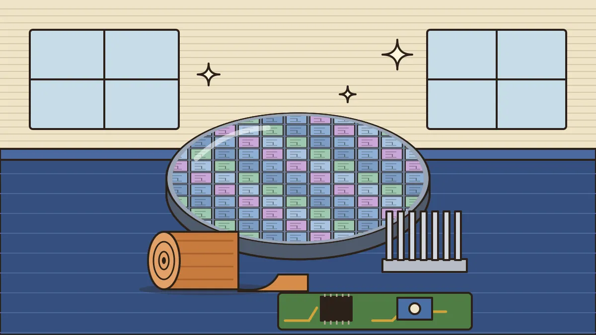
On 6 November 2026, Union Minister Shri Ashwini Vaishnaw did two things on one stage. He launched the Semicon 2.0 Web Application Portal under the Semicon India Programme, through which applications are now open for Pillars 2, 3 and 4. And he announced 12 more approved applicants under the Electronics Components Manufacturing Scheme (ECMS), with projected investment of ₹7,503 crore.
The two announcements belong together but are different things, and exam questions routinely blur them. Semicon is about the chip itself: designing it, fabricating it on a wafer and packaging it. ECMS is about everything around the chip: the circuit boards it sits on, the relays and connectors that move current, the foil, films and chemicals from which those parts are made, and the machines that make them. A phone or a laptop needs both. This article separates the two schemes and explains what each approval list actually tells us.
The day's announcements at a glance
| Item | Detail |
|---|---|
| Portal | Semicon 2.0 Web Application Portal; live for Pillars 2, 3 and 4 |
| Semicon 2.0 outlay | ₹1,27,500 crore under the India Semiconductor Mission (ISM), built on six pillars |
| ECMS approvals (this round) | 12 applications; investment ₹7,503 crore; projected production ₹39,045 crore; 7,127 direct jobs |
| Spread | 7 states: Gujarat, Karnataka, Madhya Pradesh, Maharashtra, Punjab, Tamil Nadu, Uttar Pradesh |
| ECMS cumulative | 118 applications, 34 products, 16 states, investment ₹77,051 crore, production ₹5,73,146 crore, 81,755 direct jobs |
The minister also pointed out that nearly half the units approved under ECMS are MSMEs, and set a goal for Semicon 2.0 of attracting at least three major equipment manufacturers and five chemicals and gases companies to India.
Semicon 1.0: what the first phase delivered
To judge the new phase, look at the old one. The Programme for Development of Semiconductors and Display Manufacturing Ecosystem in India was approved by the Union Cabinet in December 2021 and notified on 21 December 2021, with an outlay of ₹76,000 crore. It offers fiscal support of up to 50 per cent for silicon fabs, compound semiconductor facilities, assembly-and-test units and chip design. The India Semiconductor Mission (ISM), set up within the Digital India Corporation, runs it.
By the 6 November release, ISM had approved 12 projects across six states with cumulative investment of over ₹1.64 lakh crore. Five of them had started commercial production by October 2026. The projects, taken from Ministry replies in Parliament and Cabinet decisions, are:
| Project | State | What it makes |
|---|---|---|
| Micron (Sanand) | Gujarat | Assembly and test of DRAM and NAND memory |
| Tata Electronics with PSMC (Dholera) | Gujarat | Silicon fab, 50,000 wafer starts a month |
| Tata Electronics (Morigaon) | Assam | Advanced packaging (assembly and test) |
| CG Power with Renesas and Stars | Gujarat | Assembly and test of specialised chips |
| Kaynes Technology | Gujarat | Wire-bond and substrate-based packages |
| HCL-Foxconn joint venture | Uttar Pradesh | Display driver chips |
| 3D Glass Solutions | Odisha | Glass-substrate advanced packaging |
| SiCSem | Odisha | Silicon carbide compound fab |
| CDIL | Punjab | Power devices (MOSFETs, IGBTs) in silicon and silicon carbide |
| ASIP Technologies | Andhra Pradesh | Assembly and test |
| Crystal Matrix (Dholera) | Gujarat | Gallium nitride mini/micro-LED displays |
| Suchi Semicon (Surat) | Gujarat | Assembly and test of discrete chips |
Two points are worth a second look. First, only the Tata-PSMC project is a conventional silicon fab; most of the others are the back end (ATMP/OSAT) or compound semiconductors. That follows the logic every late-starting country uses: enter where capital needs are lower and work forward. Second, Gujarat hosts six of the twelve, which is the sort of clustering ISM has encouraged, because a packaging plant needs gases, chemicals, power and skilled people close by.
On the design side the release reports that 332 institutions received chip-design (EDA) tools under the Chips to Startup (C2S) Programme, with about 70,000 students trained, and that 105 startups have access to the tools, 24 are funded and 15 have received venture capital.
Semicon 2.0: why the portal matters
Semicon 2.0 is the second phase of the mission, with a fiscal outlay of ₹1,27,500 crore, and is organised around six pillars. We covered the pillars in detail in our explainer on Semicon 2.0's six pillars; here is the short form, with the status that changed on 6 November.
| Pillar | Focus | Applications |
|---|---|---|
| 1 | Design of chips | Not part of this launch |
| 2 | Machines and materials | Open now |
| 3 | Setting up more fabs | Open now |
| 4 | ATMP/OSAT (further strengthening) | Open now |
| 5 | Research and development | Not part of this launch |
| 6 | Talent development | Not part of this launch |
A web portal sounds like routine administration, but it matters for two reasons. It converts an announced scheme into a working application channel, which is when companies can begin to file proposals and the pipeline of approvals can start. And it covers the three capital-heavy pillars. Pillar 2 is the one to watch. A fab needs lithography tools, ultra-pure chemicals and specialty gases, which come from a handful of firms worldwide. The minister's target of three equipment makers and five chemical and gas companies is aimed at a gap the first phase left largely open: India has attracted plants, but the supply base that feeds them is still thin.
He also called for rigorous selection of projects, with quality, technological depth, R&D and global competitiveness as the tests. That points to a preference for better projects over a long list.
ECMS: the scheme behind the 12 approvals
The Electronics Components Manufacturing Scheme was notified by MeitY in April 2025 with an outlay of ₹22,919 crore over six years. Its aim is to deepen domestic manufacturing of components and their inputs. Applications opened on 1 May 2025 and the window for most product segments was extended to 30 September 2025. The response was far above target: 249 applications with proposed investment of ₹1,15,351 crore, against the scheme's goal of ₹59,350 crore of investment, production of about ₹4.56 lakh crore and 91,600 direct jobs.
Approvals come in tranches, which is why the numbers keep growing:
| Tranche | Date | Approvals | Investment |
|---|---|---|---|
| First | Oct 2025 | 7 applications | ₹5,532 crore |
| Second | 17 Nov 2025 | 17 applications | ₹7,172 crore |
| Third | 2 Jan 2026 | 22 proposals | ₹41,863 crore |
| Up to the previous list | - | 106 applications in total | ₹69,548 crore |
| This list (6 Nov 2026) | 6 Nov 2026 | 12 applications | ₹7,503 crore |
| Cumulative | 118 applications | ₹77,051 crore |
The arithmetic checks out: ₹69,548 crore plus ₹7,503 crore gives ₹77,051 crore, and 106 plus 12 gives 118.
What the 12 approvals make
The approvals cover 10 target products, in three groups.
Four components. Multi-layer printed circuit boards (NeST ICELR), relays (TDConnex, Chennai), heat sinks (Modern Automotives) and specialty ceramics (Voltix Semicon).
Five supply-chain products. Copper foil (Indo Asia Copper), anode material (TACC), cathode active material (Vidyuta Materials), polypropylene film (Enerfolie) and camera rim (Surface Modification Technologies).
Capital goods and parts. Precision moulds and tooling (TDConnex), power and control systems for capital equipment (Rockwell Automation India) and factory-automation equipment (Wipro Pari Robotics).
The release notes that this list includes first-time approvals under ECMS for copper foil, cathode active material and specialty ceramics. Understanding why those three matter is the most useful thing in the news.
- Copper foil is a thin sheet of copper. It is an input for copper-clad laminate (CCL), the base board on which printed circuit boards are made, and it is also used in lithium-ion cells. Making it at home removes a dependence one step further up the chain than the board.
- Cathode active material and anode material are the chemicals inside a lithium-ion cell, where the cathode and anode store and release lithium ions. These are the most valuable parts of a battery. Assembling cells from imported materials adds little value; making the materials adds a lot.
- Polypropylene film serves as the dielectric in capacitors. A capacitor is two conductors separated by an insulator, and the film is that insulator.
- Specialty ceramics are used in electronic components for their insulating and heat-handling properties.
The pattern is clear. The first tranches went mostly to final components, such as boards, camera modules and connectors. This one reaches back into the raw material. That is the meaning of the minister's line that India's electronics story has moved "beyond assembly" to a domestic value chain of modules, components, materials and technologies.
Why value addition is the real argument
India is now a large electronics producer. PIB figures for 2024-25 show electronics production of about ₹11.3 lakh crore, up from about ₹1.9 lakh crore in 2014-15, and mobile phone production of ₹5.45 lakh crore, with imports falling from 75 per cent of demand to a tiny fraction. But the same releases state that domestic value addition is only about 18 to 20 per cent. In other words, for each ₹100 of device, around ₹80 is still imported components and materials.
That gap is the case for ECMS. The scheme pays for production of the parts so that more of the value stays in India, and it ties in with the government's goal of a $500 billion electronics manufacturing base by 2030-31. Our explainer on the Mobile Phone Manufacturing Scheme covers the assembly-versus-value-addition debate from the device side. ECMS is the other half of the same argument, from the parts side.
Two cautions belong in a balanced answer. First, projections are not production: investment, output and jobs here are projected figures, and only the units that start commercial production count. Second, the ECMS list has many small and mid-sized firms, and the scheme's success will depend on whether they reach the quality and scale that global customers demand, which the minister himself stressed.
The industrial-policy toolkit, in one view
CDS questions on industry like to ask which instrument does what.
- Production-Linked Incentive (PLI): pays a share of incremental sales of goods made in India.
- ECMS: supports component and input manufacturing, with incentives tied to turnover and capital spending depending on the category.
- ISM / Semicon: supports capital investment in fabs and packaging, up to 50 per cent of the project cost, plus design-linked support for chip companies.
- Make in India: the umbrella programme for all of these; see our explainer on what twelve years of Make in India changed.
What to watch next
- Pillar 2 applicants. Whether named equipment, chemicals and gas companies file under the new portal, and when the first approvals are announced.
- New fabs. Whether Pillar 3 draws new fab proposals, silicon, compound or display, beyond Dholera and Odisha.
- Output, not approvals. How many of the 118 ECMS units begin production, and what happens to the 18 to 20 per cent value-addition figure.
- Back-end plants. More of the five operating ISM projects reaching volume.
🔑 Revision block
The news. 6 Nov 2026: Minister Ashwini Vaishnaw launched the Semicon 2.0 Web Application Portal; applications live for Pillars 2, 3 and 4; announced 12 approvals under ECMS.
Semicon 2.0. Outlay ₹1,27,500 crore under ISM; six pillars: Design · Machines and Materials · More Fabs · ATMP/OSAT · R&D · Talent. Target: at least 3 equipment makers and 5 chemicals and gases companies.
Semicon 1.0. ₹76,000 crore, notified 21 Dec 2021; up to 50% fiscal support; 12 projects, six states, over ₹1.64 lakh crore; 5 in commercial production (Oct 2026). Only one conventional silicon fab (Tata-PSMC, Dholera, 50,000 wafer starts/month); SiCSem (Odisha) is the silicon carbide fab; Gujarat has six projects.
ECMS. Outlay ₹22,919 crore; applications 1 May to 30 Sep 2025; 249 applications, ₹1,15,351 crore proposed. This list: 12 applications, ₹7,503 crore, ₹39,045 crore production, 7,127 jobs, 7 states, 10 products. Cumulative: 118 applications, 34 products, 16 states, ₹77,051 crore.
First-time ECMS products. Copper foil, cathode active material, specialty ceramics. Copper foil goes into CCL (PCBs) and Li-ion cells; polypropylene film is a capacitor dielectric.
The gap. Domestic value addition in electronics is only about 18-20%. Target: $500 billion electronics production by 2030-31.
Do not confuse. Semicon = chips and fabs; ECMS = components and materials; PLI = incentive on incremental sales.
🎯 Practice MCQs
Q1. The Electronics Components Manufacturing Scheme (ECMS) primarily supports:
(a) the design of semiconductor chips only
(b) the sale of imported electronic goods
(c) assembly of mobile phones from imported kits
(d) domestic manufacture of electronic components and their inputs
→ (d)
ECMS targets components, supply-chain materials and capital goods. Chip design is handled by Semicon's design pillar and the Design Linked Incentive.
Q2. Under which pillars of Semicon 2.0 did applications go live with the portal launched on 6 November 2026?
(a) Pillars 1, 2 and 3
(b) Pillars 2, 3 and 4
(c) Pillars 4, 5 and 6
(d) All six pillars
→ (b)
Applications opened for Machines and Materials, More Fabs and ATMP/OSAT. Design, R&D and Talent were not part of this launch.
Q3. The outlay of Semicon 2.0 under the India Semiconductor Mission is:
(a) ₹22,919 crore
(b) ₹76,000 crore
(c) ₹1,27,500 crore
(d) ₹62,500 crore
→ (c)
₹76,000 crore was the first phase and ₹22,919 crore is the ECMS outlay. ₹62,500 crore is the Mobile Phone Manufacturing Scheme.
Q4. Copper foil, approved for the first time under ECMS, is an input for:
(a) optical fibre and solar glass
(b) steel alloys and cement
(c) fertiliser and pesticide
(d) copper-clad laminate and lithium-ion cells
→ (d)
The foil is the base of copper-clad laminate, from which circuit boards are made, and it is used in lithium-ion cells.
Q5. Which of the following is a compound semiconductor facility among the projects approved under ISM?
(a) Micron, Sanand
(b) Tata Electronics with PSMC, Dholera
(c) SiCSem, Odisha
(d) Kaynes Technology, Gujarat
→ (c)
SiCSem will make silicon carbide devices. Micron and Kaynes are assembly-and-test units, and the Tata-PSMC unit is a silicon fab.
Q6. Consider the following statements:
1. ECMS has so far approved applications from 16 states, with a cumulative projected investment of ₹77,051 crore.
2. All the ISM-approved projects are conventional silicon wafer fabs.
Which of the statements given above is/are correct?
(a) 1 only
(b) 2 only
(c) Both 1 and 2
(d) Neither 1 nor 2
→ (a)
Statement 1 matches the 6 November release. Statement 2 is wrong: only one project, in Dholera, is a conventional silicon fab; most are packaging units or compound-semiconductor facilities.
Q7. In a capacitor, polypropylene film is used as the:
(a) electrode
(b) dielectric
(c) terminal
(d) heat sink
→ (b)
A capacitor is two conductors separated by an insulating dielectric, and capacitor-grade polypropylene film serves as that dielectric.
Q8. Domestic value addition in India's electronics manufacturing is currently estimated at about:
(a) 18 to 20 per cent
(b) 35 to 40 per cent
(c) 55 to 60 per cent
(d) 75 to 80 per cent
→ (a)
PIB puts it at roughly 18-20 per cent, which is the gap that ECMS and the material-level approvals aim to narrow.
📋 How this gets asked (PYQ pattern)
Industrial-policy questions on electronics and semiconductors arrive in four shapes.
The first is scheme matching: which scheme does what, set across PLI, ECMS, ISM and Make in India. The trap is giving the right objective to the wrong scheme, as in Q1 and Q3 above.
The second is the value-chain item: front end versus back end, fab versus OSAT, and where components and materials fall. Knowing that a fab is capital-heavy and a packaging unit is the cheaper entry point answers most of them.
The third is the material item: why silicon carbide or gallium nitride is used, what copper foil or a dielectric does. This is chemistry and physics sitting inside an economics question.
The fourth is the number item: outlays, project counts and states. For this cycle the hooks are ₹1,27,500 crore (Semicon 2.0), ₹22,919 crore (ECMS), 118 applications across 16 states, and 12 ISM projects in six states. We describe the recurring pattern, not any specific past question.
Preparing for CDS? Keep a one-page table of the schemes (PLI, ECMS, Semicon, Mobile Phone Manufacturing) with their purpose and outlay, since examiners set them against each other. Revise the basics through our notes on industry and services, follow the daily CDS current affairs, and learn with experienced faculty in the upcoming Cavalier courses in Delhi.
Source: PIB / Ministry of Electronics & IT, "Union Minister Ashwini Vaishnaw Launches Semicon 2.0 Web Application Portal and Announces 12 Approved Applicants under Electronics Components Manufacturing Scheme", 6 November 2026; MeitY releases on ECMS tranches (17 November 2025, 2 January 2026) and applications (2 October 2025); Lok Sabha reply of 1 April 2026 and Cabinet release of 5 May 2026 on ISM projects; PIB Backgrounder on ISM 2.0, 7 February 2026. The ECMS notification date was cross-checked with independent sources.
✍️ Written by Aditya Tiwari — Economy & current-affairs faculty at The Cavalier. Reviewed by the Cavalier Faculty Desk.