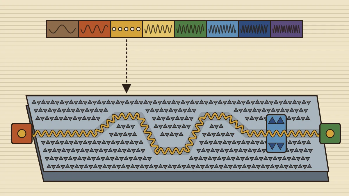
Each generation of mobile network has moved to higher radio frequencies, because higher frequencies leave room for more data. The next step, 6G, is expected to go beyond the microwave range into the terahertz band. That raises a plain engineering problem: how do you steer such short waves around a chip without losing them at every bend?
On 4 November 2026, the Press Information Bureau reported an answer from researchers at the Jawaharlal Nehru Centre for Advanced Scientific Research (JNCASR), an autonomous institute of the Department of Science and Technology (DST). They have built a silicon chip that lets terahertz waves cross a deliberately placed barrier with only about 1–2% loss, while carrying data at up to 100 gigabits per second (Gbit/s). The work appears in the journal Advanced Materials. This article starts from the physics, because the news only makes sense once the spectrum is clear.
The electromagnetic spectrum, and where terahertz sits
Light, radio and X-rays are all electromagnetic waves. They travel at the same speed in vacuum, about 3 × 10⁸ metres per second, and differ only in frequency (f) and wavelength (λ), which are tied by the relation c = f × λ. Higher frequency means shorter wavelength and more energy per photon.
| Band | Rough wavelength | Familiar use |
|---|---|---|
| Radio waves | metres to kilometres | Broadcasting, navigation, older mobile networks |
| Microwaves | about 1 mm to 1 m | Radar, Wi-Fi, 4G and 5G, microwave ovens |
| Terahertz | about 0.03 mm to 3 mm (0.1–10 THz) | Research, security imaging, future 6G |
| Infrared | about 700 nm to 1 mm | Remote controls, thermal cameras, optical fibre |
| Visible light | about 400–700 nm | Vision |
| Ultraviolet | about 10–400 nm | Sterilisation, the Sun's tanning rays |
| X-rays | about 0.01–10 nm | Medical imaging |
| Gamma rays | shorter than about 0.01 nm | Radioactive decay, cancer therapy |
The band edges are conventions and overlap a little, but the order is fixed, and the order is what exams ask. Remember it as radio, microwave, infrared, visible, ultraviolet, X-ray, gamma, with terahertz tucked between microwave and infrared. Our notes on optical phenomena and modern physics cover the waves on either side.
One terahertz is 10¹² hertz, a thousand gigahertz. The chip was measured across 310–360 GHz. A wave at 335 GHz, in the middle of that range, has a wavelength of about 3 × 10⁸ ÷ 3.35 × 10¹¹, which is roughly 0.9 mm. These waves are about a millimetre long, so a circuit that guides them can be small enough to sit on a chip.
Why was it called the "terahertz gap"?
For decades this band was awkward from both sides. Electronic circuits, which work well up to the microwave range, struggled to make and amplify signals at terahertz frequencies. Optical devices, which work well from the infrared upwards, struggled at the long-wavelength end. Sources, detectors and, above all, waveguides for the gap were hard to build, so it earned the nickname. Much recent research has been about closing it.
Why 6G wants terahertz
The reason is bandwidth, the width of the frequency slice a signal can use. The maximum data rate of a channel grows with its bandwidth, so wider channels carry more data.
| Generation | What it added | Typical channel width |
|---|---|---|
| 1G | Analogue voice | Narrow, tens of kHz |
| 2G | Digital voice and SMS | Hundreds of kHz |
| 3G | Mobile data | A few MHz |
| 4G (LTE) | Mobile broadband | Up to 20 MHz per carrier |
| 5G | Very high speed, low delay | Up to 100 MHz in mid-bands and 400 MHz in millimetre-wave bands |
| 6G (expected around 2030) | Terahertz links, sensing | Possibly many gigahertz |
At terahertz frequencies, a channel can be tens of gigahertz wide, hundreds of times wider than a 5G channel. That is why researchers talk about 6G speeds of the order of a terabit per second. India has been preparing for this: the Bharat 6G Vision document was unveiled by the Prime Minister on 22 March 2023, together with a 6G test bed, and our articles on India's 6G Call to Action and the Bharat 6G Symposium on standard-essential patents cover the policy side. The chip in the news belongs to the hardware side.
The catch is physical. Short waves are absorbed by water vapour in the air and blocked by walls, so terahertz links over any distance are difficult. The practical gain is therefore for short, ultra-fast links and for circuits inside devices, where the signal must be routed on a chip. That is where bends and obstacles do their damage.
The problem on the chip: reflections
A waveguide is a path that confines a wave. On a chip, a waveguide is a strip of material. The trouble comes when the path bends sharply, splits, or meets a change in geometry. At each such point, part of the wave is scattered or reflected backwards. This is backscattering, and the lost signal never reaches its destination. In a conventional waveguide, a barrier in the path "markedly reduces transmission", as the release puts it.
The solution: a crystal of holes, and a topology trick
The JNCASR team used three ideas stacked together.
1. A photonic crystal. A photonic crystal is a material with a regular pattern of holes or other repeating structure, on the scale of the wavelength. Just as the regular arrangement of atoms in a semiconductor creates energy bands for electrons, the regular pattern in a photonic crystal creates bands for light, including ranges of frequency that cannot pass through at all (a photonic band gap). Here the pattern is triangular holes in a silicon slab.
2. A guided boundary. When two regions of the crystal have patterns that are, in a sense, mirror versions of each other, a wave can travel along the boundary between them. This boundary channel is the waveguide. The release says such channels "resist certain kinds of backscattering".
3. A honeycomb like graphene. The crystal was designed so that its structure mimics the honeycomb lattice of graphene, the one-atom-thick carbon sheet whose discovery earned the 2010 Nobel Prize in Physics. The field is called topological photonics, borrowing from topological phases of matter (the subject of the 2016 Nobel Prize in Physics). The key idea is that some properties are protected by the shape of the arrangement, so small imperfections do not destroy them. That robustness is exactly what a waveguide needs.
Photonic Klein tunnelling
The release names the effect: photonic Klein tunnelling. In quantum physics, a particle meeting a barrier normally has only a small chance of getting through, and the chance falls fast as the barrier grows. Klein tunnelling, named after physicist Oskar Klein (1929), is the surprising exception for certain relativistic particles, which can pass through a high barrier with little reflection. It was famously predicted for electrons in graphene. The JNCASR team has shown a photonic version: the barrier is made by simply changing the sizes of the triangular holes over a short section of the waveguide, yet the terahertz wave goes through with very little loss.
The release also gives a design rule. Transmission stayed close to its barrier-free level as long as the barrier strength stayed below a characteristic coupling strength of the crystal. Since the barrier is set by hole geometry, an engineer can choose it on purpose.
What the experiment showed
The team fabricated three devices on high-resistivity silicon, which is compatible with established semiconductor manufacturing, and measured them across 310–360 GHz. The results agreed closely with simulation.
| Device | What it tested | Data rate |
|---|---|---|
| Two barriers in sequence | Loss from repeated obstacles | 48 Gbit/s |
| Omega-shaped route with four sharp bends and a central barrier | Bends plus a barrier | 60 Gbit/s |
| Power splitter with a barrier in one branch | Routing and splitting | 100 Gbit/s |
Key numbers to hold on to:
- One barrier added only about 1–2% loss; two barriers in sequence about 2–3%.
- In the splitter, the two outputs were nearly identical, so the barrier barely affected transmission.
- The splitter carried 100 Gbit/s using QAM-32. QAM is quadrature amplitude modulation, a way of encoding data in both the amplitude and phase of the wave. With 32 distinct states, each symbol carries 5 bits (2⁵ = 32).
What 100 Gbit/s means in a daily setting
The release makes a comparison: a 5-gigabyte high-definition film could in principle be transferred in under half a second. Check it. One byte is 8 bits, so 5 GB is 40 gigabits, and 40 ÷ 100 = 0.4 seconds. Watch the units, because Gbit/s is bits per second and GB is bytes. The mix-up between the two is a classic exam trap.
Who did it
- The study was led by Dr Abhishek Kumar, Assistant Professor at JNCASR, who heads the Meta Optics Laboratory (MetoLab). Samina Mulla and Sangram Kumar Sadhu of JNCASR are joint first authors.
- Collaborators came from IISER Kolkata, IIT Bombay, the Institute of Microelectronics at A*STAR, Singapore, and the University of Lille and CNRS, France.
- JNCASR, in Bengaluru, is an autonomous institute of the Department of Science and Technology, founded in 1989. DST sits in the Ministry of Science and Technology.
- The paper is in the journal Advanced Materials.
The team's next step is to tune the barriers electrically, thermally or mechanically. A tunable barrier could redirect a signal between paths on demand, turning a passive chip into a switch.
How far is this from your phone?
It is still a laboratory demonstration. A chip that works on a test bench at 310–360 GHz is not a base station or a handset, and 6G standards are still being written. What the work offers is a design tool: a way to build terahertz circuits that route and split signals on one chip without losing them at bends. Its compatibility with ordinary silicon manufacturing is the encouraging part, because circuits made that way can in principle be produced at scale.
For defence-minded readers, terahertz technology is also studied for security imaging and high-resolution sensing, and secure, very high-speed links are a military need. These are research directions, not claims of the present release, which speaks only of 6G.
How to hold this together for the exam
Think in three layers.
- The spectrum. Know the order of the bands and where terahertz sits.
- The generation story. Know why each generation moved to higher frequencies (bandwidth) and what limits terahertz (absorption and blockage).
- The device idea. Know the vocabulary: photonic crystal, waveguide, backscattering, topological photonics, Klein tunnelling.
Our notes on magnetism and electromagnetic effects help with the underlying field concepts.
🔑 Revision block
The news. PIB, 4 November 2026: a silicon chip from JNCASR (autonomous institute of DST, Bengaluru, founded 1989) guides terahertz waves across an engineered barrier with 1–2% loss (2–3% for two barriers), carrying up to 100 Gbit/s. Published in Advanced Materials.
Spectrum order. Radio, microwave, terahertz, infrared, visible, ultraviolet, X-ray, gamma. c = f × λ; 1 THz = 10¹² Hz; measured range 310–360 GHz (wavelength about 0.9 mm).
Why terahertz. Wider bandwidth means more data. 4G up to 20 MHz per carrier; 5G up to 100 MHz (mid-band) and 400 MHz (millimetre wave). 6G expected around 2030. Bharat 6G Vision: 22 March 2023. Short waves are absorbed by water vapour and blocked by walls.
The device. Photonic crystal: triangular holes in silicon, mimicking graphene's honeycomb lattice. Waves run along the boundary between two regions and resist certain backscattering (topological photonics). The barrier is made by changing hole sizes: photonic Klein tunnelling.
Test devices. Double barrier 48 Gbit/s; omega route (four bends plus barrier) 60 Gbit/s; splitter 100 Gbit/s with QAM-32 (5 bits per symbol). 5 GB film in about 0.4 s.
People and next step. Dr Abhishek Kumar (MetoLab, JNCASR); partners IISER Kolkata, IIT Bombay, ASTAR Singapore, Lille and CNRS. Next: tunable* barriers (electrical, thermal, mechanical).
🎯 Practice MCQs
Q1. In the electromagnetic spectrum, terahertz waves lie between:
(a) Radio waves and microwaves
(b) Microwaves and infrared light
(c) Infrared and visible light
(d) Ultraviolet and X-rays
→ (b)
Terahertz frequencies (about 0.1–10 THz) sit between microwaves and infrared light, which is why the band was long called the terahertz gap.
Q2. The Jawaharlal Nehru Centre for Advanced Scientific Research, whose team built the terahertz chip, is an autonomous institute under the:
(a) Council of Scientific and Industrial Research
(b) Defence Research and Development Organisation
(c) Department of Science and Technology
(d) Ministry of Education
→ (c)
JNCASR is an autonomous institute of the Department of Science and Technology.
Q3. If a chip carries data at 100 gigabits per second, a 5-gigabyte film can in principle be transferred in about:
(a) 0.4 second
(b) 4 seconds
(c) 40 seconds
(d) 400 seconds
→ (a)
5 gigabytes is 40 gigabits (8 bits per byte), and 40 ÷ 100 = 0.4 second. The news release describes this as under half a second.
Q4. The Bharat 6G Vision document was unveiled in:
(a) 2020
(b) 2021
(c) 2022
(d) 2023
→ (d)
It was unveiled on 22 March 2023 along with a 6G test bed.
Q5. Consider the following statements about the terahertz chip:
1. Terahertz radiation is ionising in the same way as X-rays.
2. The chip uses a pattern of triangular holes in a silicon slab.
Which of the statements given above is/are correct?
(a) 1 only
(b) 2 only
(c) Both 1 and 2
(d) Neither 1 nor 2
→ (b)
Terahertz photons carry far less energy than X-rays and are non-ionising, so statement 1 is wrong. The device is a photonic crystal made of triangular holes in silicon.
Q6. In the demonstration, the 100 Gbit/s link used QAM-32. Each symbol in QAM-32 carries:
(a) 2 bits
(b) 4 bits
(c) 5 bits
(d) 32 bits
→ (c)
With 32 distinct states, each symbol carries log₂32 = 5 bits.
Q7. The devices in the JNCASR experiment were fabricated on high-resistivity:
(a) Gallium arsenide
(b) Germanium
(c) Glass
(d) Silicon
→ (d)
High-resistivity silicon is compatible with established semiconductor manufacturing, which makes scaling plausible.
Q8. The photonic crystal in the chip was designed to mimic the lattice of graphene, which is:
(a) Honeycomb
(b) Body-centred cubic
(c) Face-centred cubic
(d) Simple square
→ (a)
Graphene is a single layer of carbon atoms in a honeycomb arrangement.
📋 How this gets asked (PYQ pattern)
Science-and-technology questions in the NDA general ability paper tend to come from three directions, and this news touches all of them.
The first is physics basics through a news hook: the order of electromagnetic waves, the relation between frequency and wavelength, or which wave is used for what. Q1 above is the pattern. Expect options that swap neighbouring bands.
The second is technology generations and communication: what 4G, 5G and 6G add, and the units used (hertz, bits per second). Option sets often mix bits with bytes or megahertz with gigahertz.
The third is institutions and people: which body owns which institute (DST, CSIR, DRDO, ISRO) and which ministry sits above it. Q2 is built that way.
Preparing for NDA? Learn the electromagnetic spectrum as one ordered list and practise a few frequency-to-wavelength conversions with c = f × λ. Revise the topic with our notes on optical phenomena, then browse the full NDA study material, follow the daily NDA current affairs, and learn with experienced faculty in the upcoming Cavalier courses in Delhi.
Source: PIB / Ministry of Science & Technology, "Novel silicon chip allowing terahertz waves to pass through barriers could enable future 6G networks", 4 November 2026 (study published in Advanced Materials). Bharat 6G Vision date from press reports of the 22 March 2023 launch. Background on the spectrum, channel widths and Klein tunnelling is standard physics; the 0.4-second and 0.9 mm figures are calculated by The Cavalier.
✍️ Written by Col D.N. Sharma — Science & general-studies faculty at The Cavalier. Reviewed by the Cavalier Faculty Desk.